Sort by

Newest

Oldest

Popular

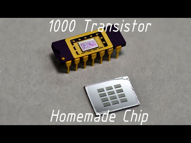
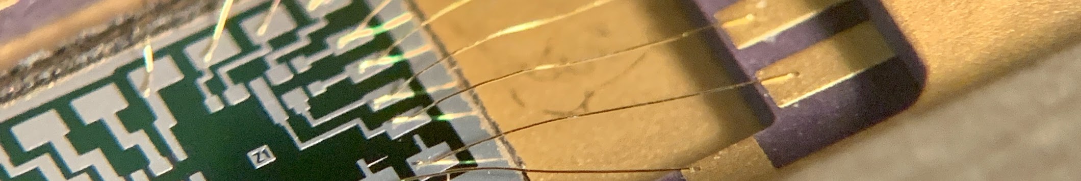
"Z2" - Upgraded Homemade Silicon Chips
05:46
Etching Silicon with Plasma - Reactive Ion Etching (RIE)
11:40
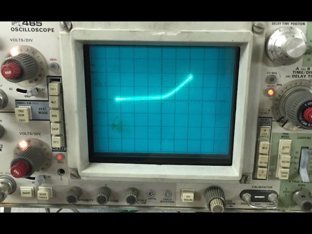
MOS Capacitance/Voltage (C-V) Measurement
14:14
Maskless Photolithography Stepper for Homemade Chips
09:41
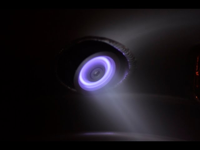
High energy particle mirror
04:19
Counting Atoms with the Doppler Effect - Heterodyne Interferometer
16:25
Simple Thin Film Thickness Measurement with Spectrometer
07:55
"Z1" - Homemade Silicon ICs / Computer Chips
02:22
Wire Bonding Basics - Manual Wedge Bonding ICs
13:20
Making Tiny Things with Electron Microscope - E-beam Lithography
08:44
Energy Dispersive X-ray Spectroscopy (EDS) with Silicon Drift Detector (SDD) Theory and Demo
27:15
SEM Optimization, Astigmatism Correction, and Basic Electron Optics
19:25
RGA Residual Gas Analyzer (Mass Spectrometer) Experiments and Helium Leak Checking
16:20
Inductively Coupled Plasma Photoresist O2 Ashing/Descum
02:31
Photonic Bandgap Nanostructures - Butterfly Wing SEM Imaging
07:30
High Vacuum Chamber Basics, Part 2 - Atmospheric to 1e-6 Torr Pumpdown Procedure
09:42
SEM Startup Procedure and Demonstration - Electron Microscopy In The Garage
22:30
Ion sputter/getter pump (UHV)
01:01
Electron Microscope Moving Montage
02:23
High Vacuum Chamber Basics, Part 1
16:51
Maskless Photolithography with DLP Projector - 10um Feature Sizes
23:06
Semiconductor Fabrication Basics - DIY Homemade NMOS FET/MOSFET/Transistor Step by Step
29:45
Semiconductor Fabrication Basics - Home Chip Lab Tour
14:08
Semiconductor Fabrication Basics - Thin Film Processes, Doping, Photolithography, etc.
48:18
mosfet gate capacitance demo
00:28
Homemade Photovoltaics - DIY Silicon PN Junction Solar Cell Testing
12:11
Homemade Silicon PN Junction Diode Test
02:04
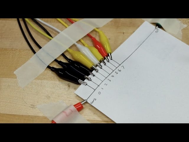
DIY Arduino Paper R2R Ladder DAC 8 bit
05:49
Opening a furnace at 2000 degrees F (1100 deg. C)
00:28
Thermal Oxide Growth on Silicon Wafer - 500nm
02:54